Services
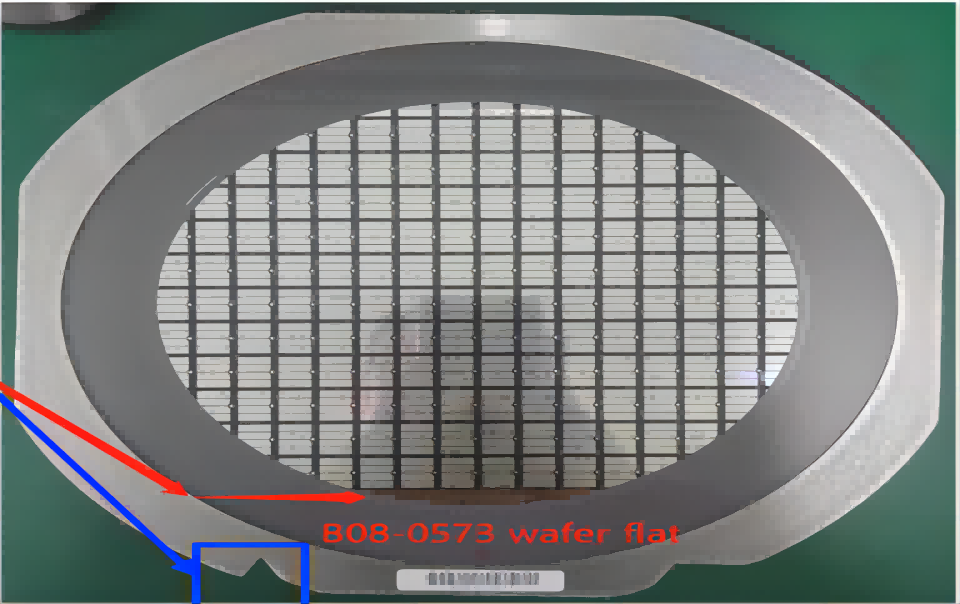
We extend our gratitude to our partners for their unwavering support over the years. Together, we are committed to continuous progress, fostering strong relationships, and collaborating for mutual development and future success.
With over a decade of experience, PlutoChip takes pride in its professional foundry services in semiconductor technology. Our design and process expertise spans a wide range of fields, including MEMS sensors, diodes, thyristors, HETMs, VCSELs, biochips, optoelectronic chips, RF chips, power devices, and WLCSP.
With our experienced design and process team, we are equipped to deliver comprehensive technical and foundry services, including customized design and development, foundry services, process validation, and packaging testing for system solutions.
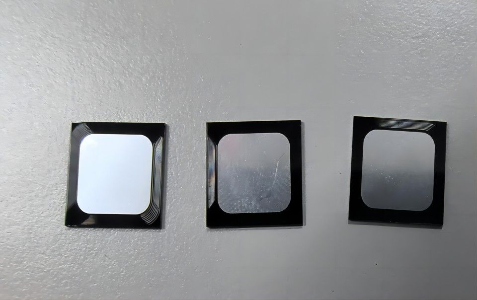
As a technology company dedicated to the design and processing of MEMS chips and discrete devices, PlutoChip boasts abundant foundry resources. We offer a full range of processing capabilities for 4-, 6-, 8-, and 12-inch wafers, adhering to 0.5μm to 3μm standards, as well as various single- or multi-step processes.
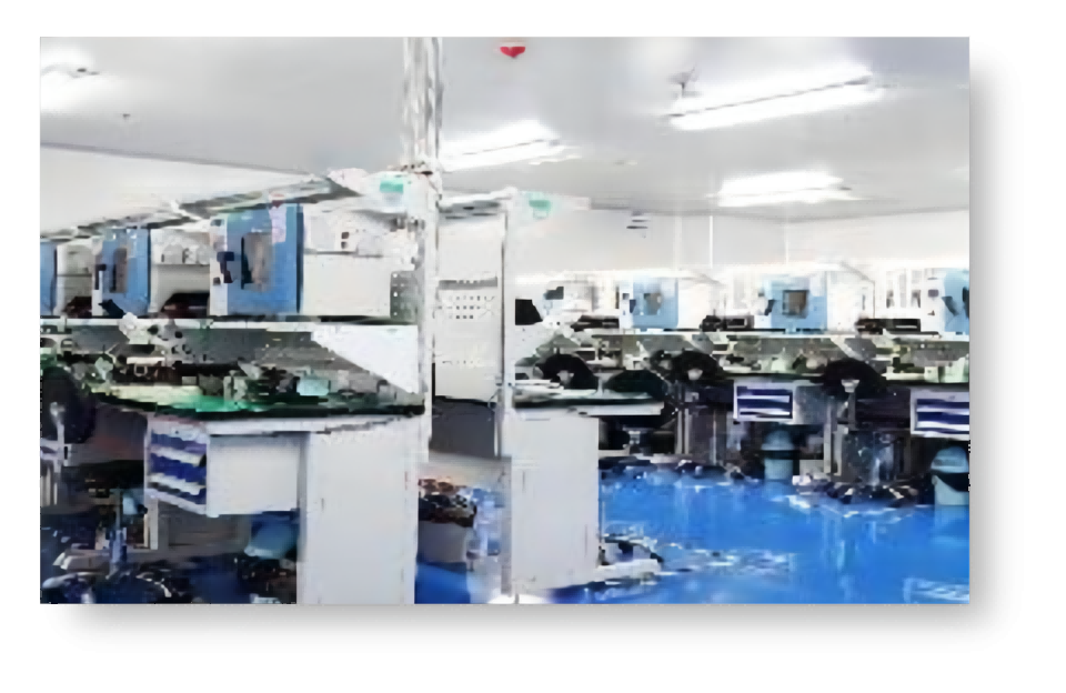
Our capabilities include mature lithography, etching, plating, wafer-level packaging, testing, and other advanced equipment that deliver excellent performance and stable processes.
We are committed to the development of our unique processes and services, enabling us to provide both standard and customized solutions to meet the specific needs of our clients. At PlutoChip, we place great importance on collaborating with small and medium-sized clients and are eager to grow together with them. Our dedication to providing outstanding services and expertise makes us a reliable partner for all your semiconductor technology needs.
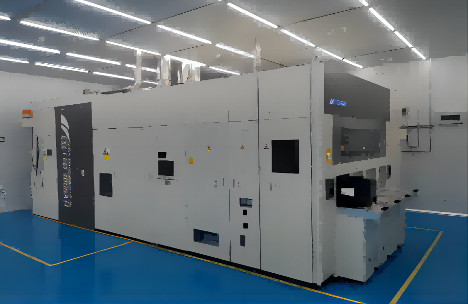
Process Foundry:
1. Lithography: SUSS-MA8; Nikon-I7/10/12; DWL-66; Elionix ELS7000;
2. Coating: EBX-1000; Denton 550; PICOSUN/SUNALETM R-200; LPCVD; Plasmalabsystem 100; Plasmalabsystem ICP380; Optorun OTFC-900;
3. Etching machine: SPTS-ICP; Oxford Plasmalab System 100 ICP180; Tegal 903E; OXFORD Ionfab 300Plus; VHF; FEL/Helios NanoLab 600i; Plasma:class-1;
4. Encapsulation: SUSS/SB6 Gen2; Disco-3350; Nilmt; TSV; NV-GSD-HE
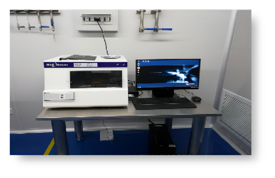
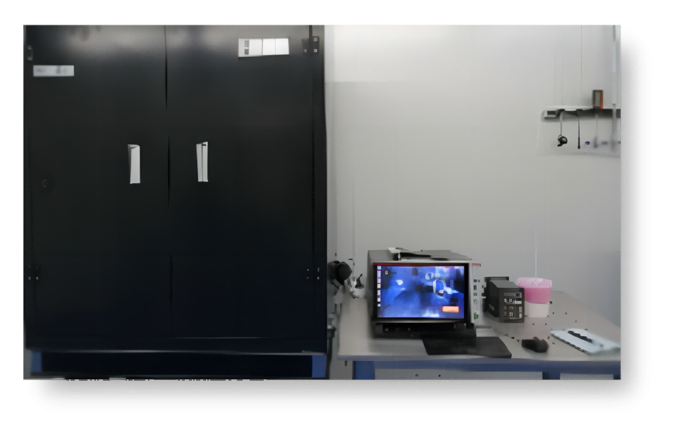
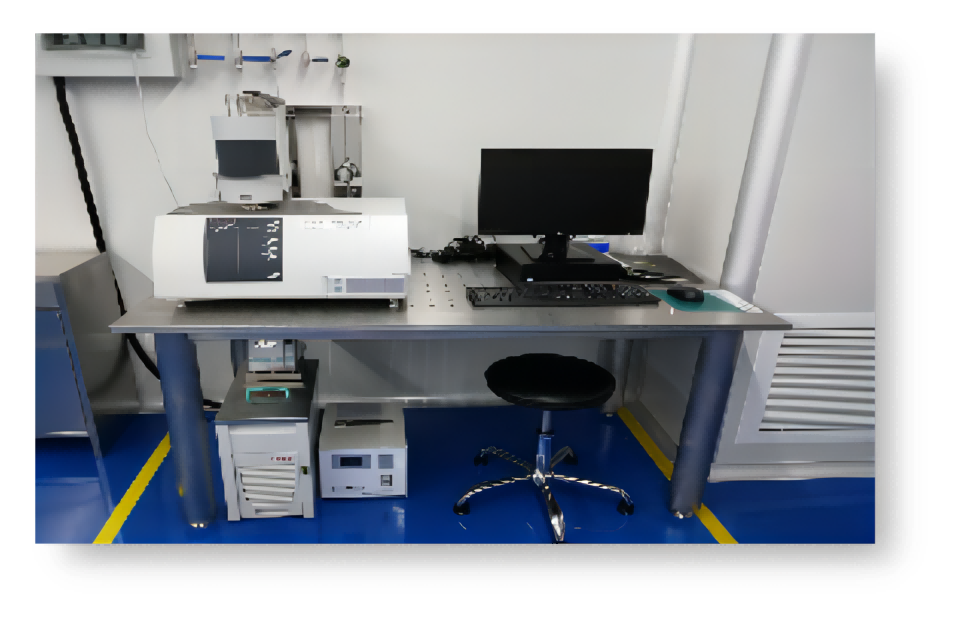
5. Detection and Testing: SU8020; VEECO; AFM;HORIBA/LabRAM HR Ecolution; K-mac
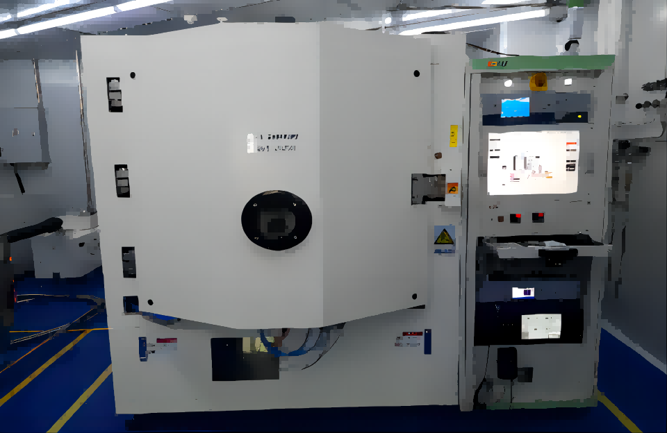
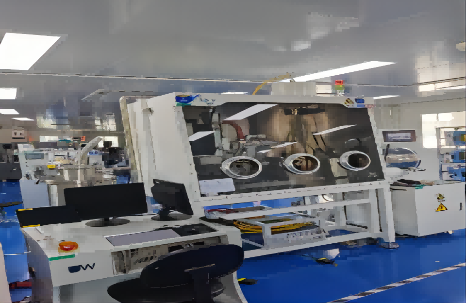
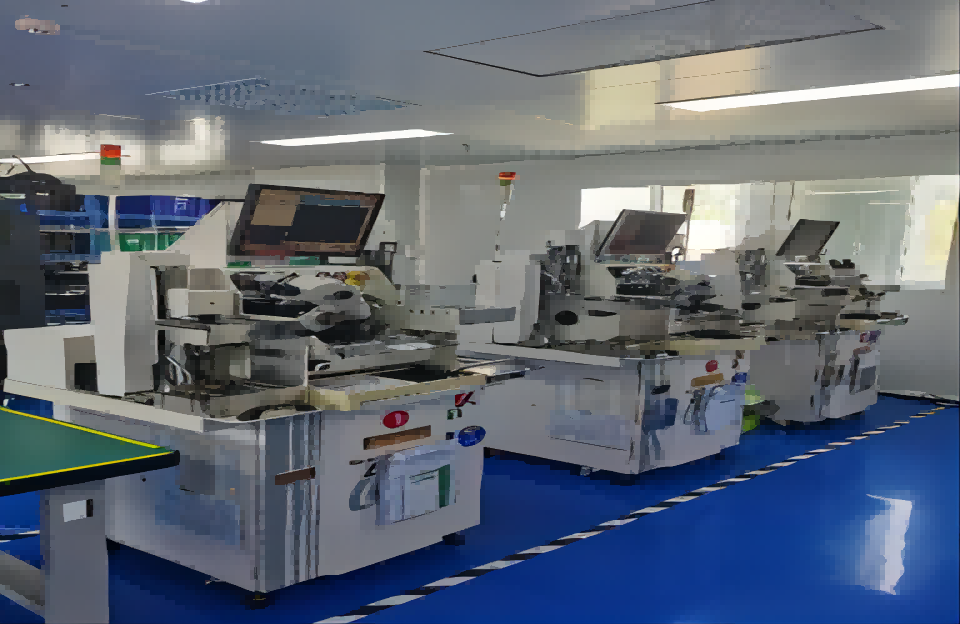
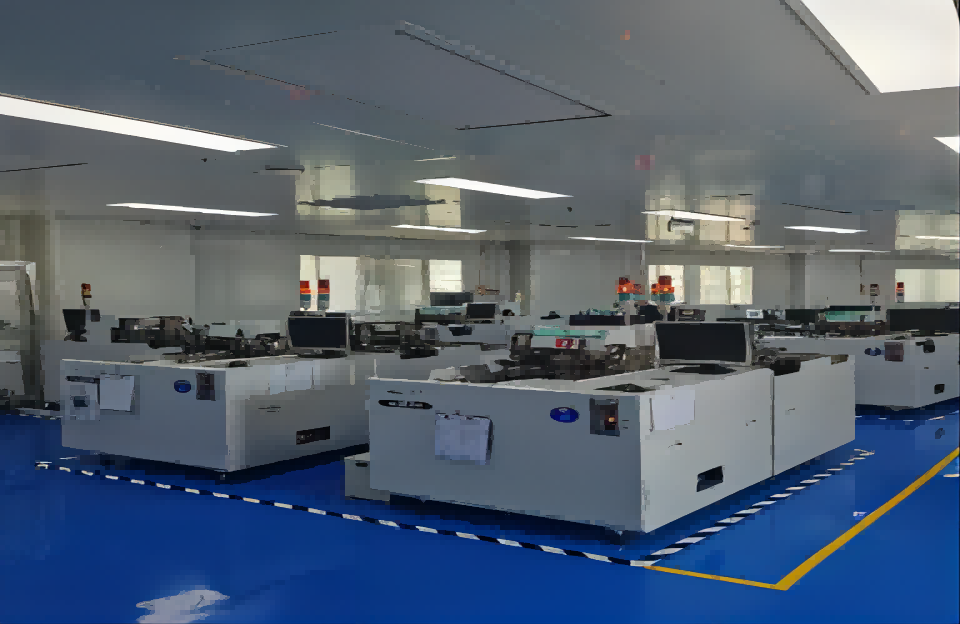
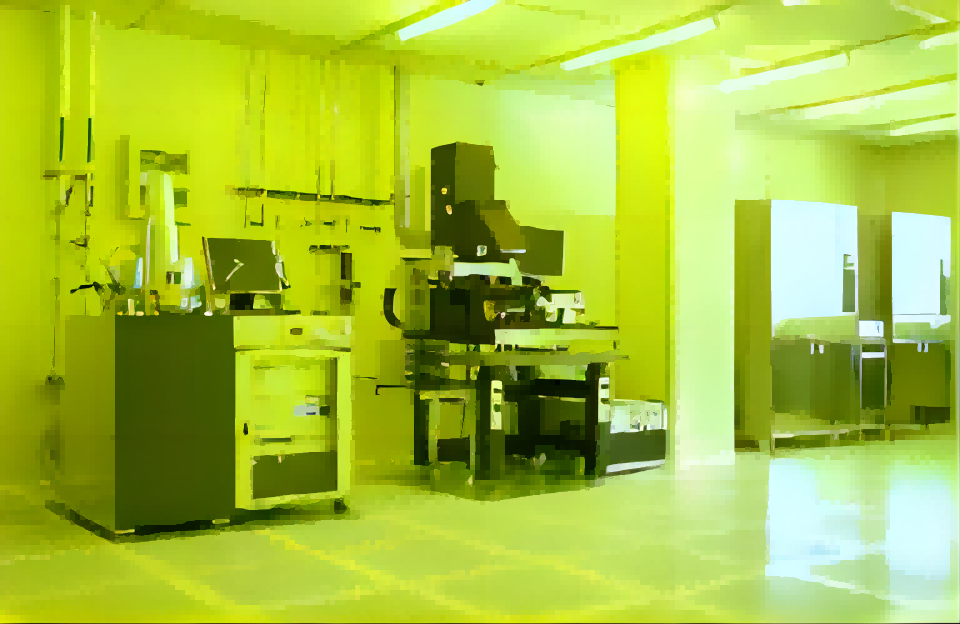
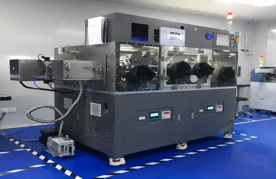
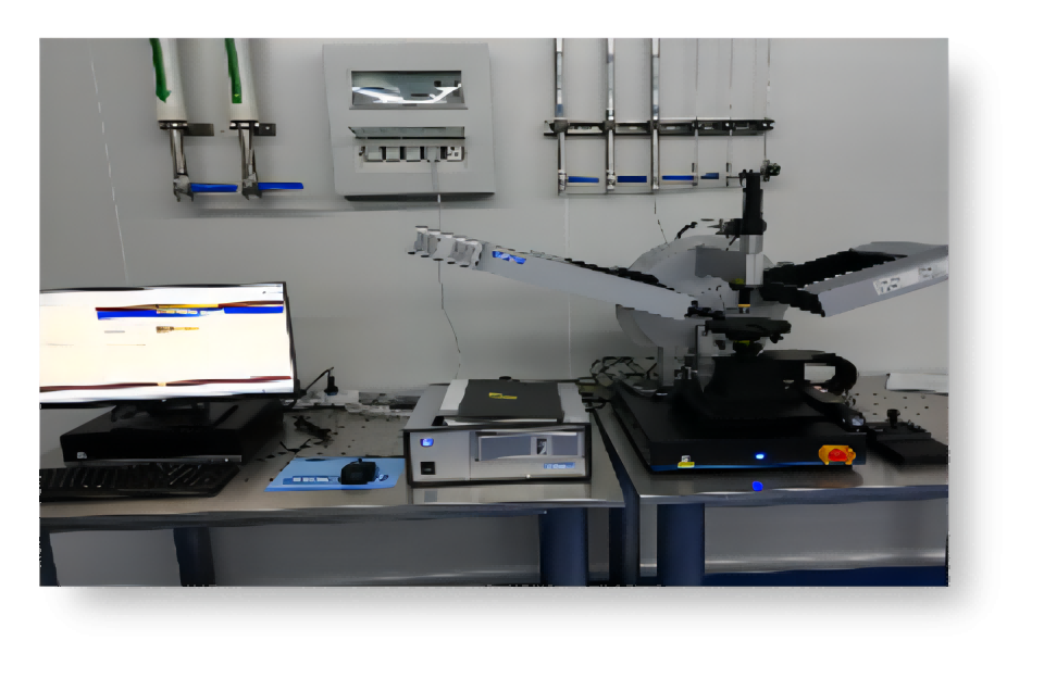
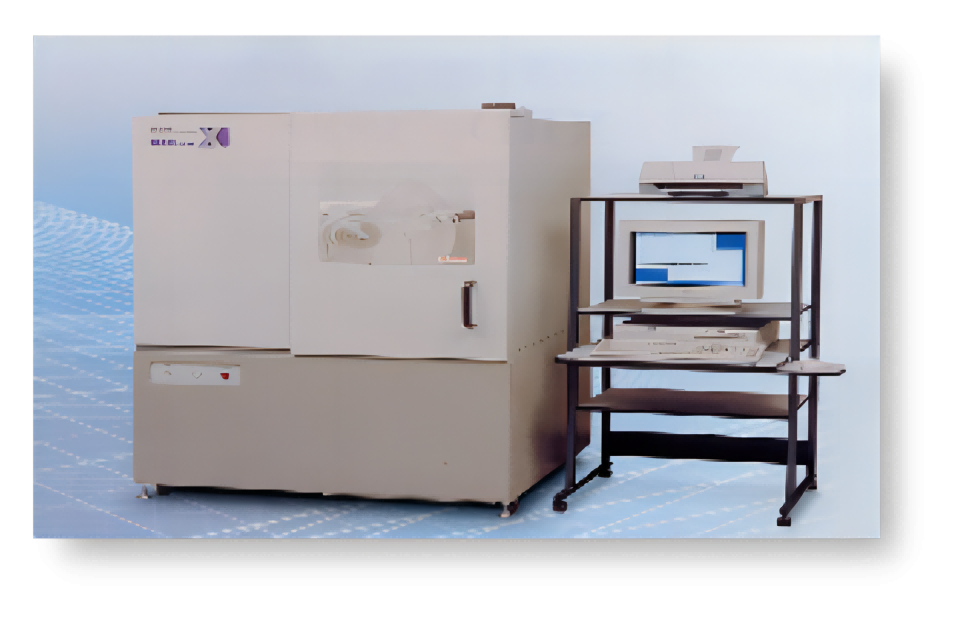
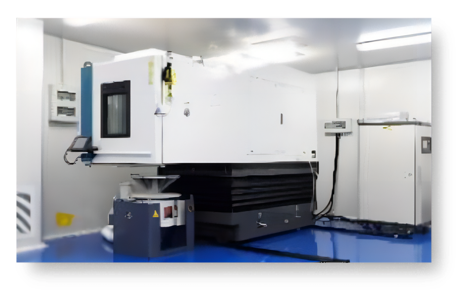
u Testing equipment: Atomic force microscope, electron scanning electron microscope, XRD, step meter, ellipsometer, thermogravimetric analyzer, Chip Probe(CP), precision electric probe table, etc
Process of Foundry Service
Make a Request
Product idea & Technical discussion
01
Specification Confirmed
Design, Discusstion, practice
02
Trial Production
Trial production of new products Evaluate Feedback
03
Prepare for mass production
Confirm mass producion Production plan
04
Mass Production
Mass Production
05
Call Us
+86 0757-8625 1566
+86 159 8906 6199
Our Email
sales@plutochip.comOur Address
Head Office:Rm 1815, Building 3, CML Center, No. 26 Guilan North Rd, Nanhai District, Foshan City, China Factory:Wanma Industries Park, Gaoming District, Foshan City, China